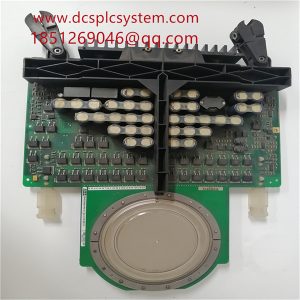
Description
The SPHSS03 is a three-channel, 200 MHz, 16-bit A/D, with a multi-band digital down-converter (DDCS) and a digital up-converter (DUC) to two 800 MHz 16-bit D/AS, XMC modules based on the XilinxKINTX Ultra Scale Fuel Component Board Assembly, which can be used in a number of applications. the SPHSS03 is designed for engineers to Digital Radio Frequency Memory (DRFM) applications, in which multi-channel inputs can digitise the incoming RF input signal over a bandwidth of up to 80 MHz, and then generate the processed RF signal as an analogue output with very low deterministic delay.
For DRFM radar applications, the received radar pulses are digitised and sent to an FPGA, which can apply a series of DSP algorithms before sending the modified signal back to the radar to simulate the reflected pulses. These algorithms are designed to confuse, deceive or disable the radar depending on the mission objectives. As a consistent representation of the original signal, the transmitting radar will not be able to distinguish it from other legitimate signals received and processed as targets. If the signal is stored in memory, it can be used to create false range targets behind (reactive jamming) and in front (predictive jamming) of the target. Slight modifications are made in the frequency analogue Doppler shift to create false target velocities.The DRFM can also be used to create distorted phase fronts, which are necessary to counter the single-pulse radar angular measurement technique.
The front end of the SPHSS03 accepts three analogue HF or if inputs on the front panel SSMC connector with converters coupled to three Texas Instruments AdS5485200 MHz, 16-bit A/D converters. These digital outputs are routed to the KINTX hyperscale FPGA for signal processing, data capture and routing to other module resources. A TIDAC5688DUC (digital upconverter) and a D/A accepted an actual or complex baseband data stream from the FPGA and provided inputs for upconversion, interpolation, and dual D/A layers.
The SPHSS03 has three A/D acquisition IP modules for easy capture and movement of data. Each IP module can receive data from any of the three A/DS or test signal generators. The powerful linked-list DMA engine moves A/D data through the PCE interface in a unique capture gate drive mode. In this mode, the length of the transfer performed through the link definition does not need to be known prior to data acquisition; instead, it is governed by the acquisition gate length. This is extremely useful for applications where external gates drive acquisition and the exact length of the gate is unknown or may change. In each A/D acquisition IP module, there is a powerful DDCIP core. Due to the flexible input routing of the A/D acquisition IP modules, many different configurations are possible, including one A/D driving two DDCs or two A/DS driving their own DDCs.


