Description
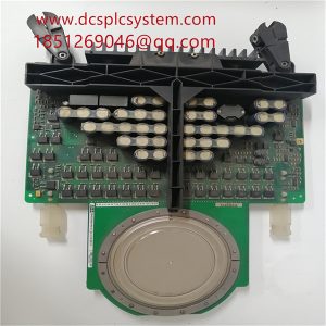
D685A1156U01 Backplane Type4 FET/FEP
D685A1156U01 will be weak signal circuits and easy to produce noise pollution circuit separate wiring, the most basic requirement is that the signal line must be and strong power control lines, power lines separate wiring, and to maintain a certain distance between each other. Wiring should be differentiated between separate AC lines, DC regulated power lines, digital signal lines, analog signal lines, inductive load drive lines. The larger the wiring interval, the shorter the wiring, the smaller the noise impact. However, the space inside and outside the actual equipment is limited, the wiring interval can not be too large, as long as the minimum interval distance can be maintained.

D685A1156U01 typical isolation transformer schematic diagram. It is the principle of anti-interference on the primary side of high-frequency interference presents a very high impedance, and is located between the primary and secondary windings of the metal shielding layer and blocked a, the secondary side of the distributed capacitance, so the primary winding is only on the shielding layer of the distributed capacitance exists, the high-frequency interference through the distributed capacitance is bypassed into the ground. 1:1 isolation effect is good or bad, often depends on the shielding layer of the process. It is best to use 0.2mm thick pure copper sheet, the primary side, the secondary side each with a shielding layer.

D685A1156U01 the primary side of the shield through a capacitor and the secondary side of the shield layer connected together, and then connected to the secondary side of the ground. It is also possible to connect the shielding layer of the primary side to the ground of the primary side and the shielding layer of the secondary side to the ground of the secondary side. And the cross-sectional area of the grounding lead should also be larger good. 1:1 isolation also effectively isolate the common mode interference of the ground loop.